
Hiro Quibbler: CMOS v CCD
Posted on Mar 29, 2010 by Alex Fice
Which is better CMOS or CCD?Film and television are, perhaps, two of the few places where C.P. Snow’s ‘Two Cultures’ actually do communicate. An extraordinary amount of science and technology is required to produce these defining art forms of the 20th Century. Albert Einstein is best known, of course, for a couple of theories of relativity, but this work was far too controversial at the beginning of the last century for an physician called Allvar Gullstrand, an influential member of the Nobel Committee. So, despite 60 or so nominations for relativity, in 1922 the Royal Swedish Academy of Sciences awarded Einstein the 1921 Nobel Prize for his discovery of the law of the photoelectric effect, kind of as a consolation prize – we can thank a virtually unknown physicist called Carl Wilhelm Oseen for brokering that particular deal. Einstein gave the considerable sum of money he received to his ex-wife.
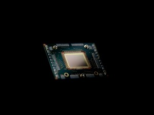
Albert’s Nobel prize winning theory gets to help the modern day image-maker too. Imaging sensors use a variation of the photoelectric effect he described and here, too, there are developing two cultures – those who follow the Charge Coupled Device (or CCD) and those true believers in CMOS.
The first step in either type of imager is to convert the light (photons) falling onto the chip into an electric charge (electrons). This requires a lot of difficult quantum mechanical calculations, so you can thank Einstein that he started the ball rolling with the sums. Fortunately, the photon’s don’t care – they hit some silicon and raise the energy of some of its electrons enough to free them and we have our charge. The more light that hits the silicon, the more electrons we get. A bigger bit of silicon (i.e. a bigger light sensitive area) will give us more charge for a given intensity of light as there are more photons hitting its surface – like the difference between catching rain in a sail or in a handkerchief. In principle, both CCDs and CMOS sensors convert photons to electrons the same way – the differences come in what happens to the electrons afterwards, and in the implications that has to the way the chip are made.
The little light sensitive pixels (photosites) in our sensor will continue to convert photons to charge as long as light falls on them, which is why digital stills cameras still tend to have mechanical shutters. The CCD’s electronic shutter works by transferring the charge in each pixel to a storage bin next to the light sensitive area. The chips are arranged so that charge can be passed from bin to bin until it gets to an amplifier at the edge of the chip where the charge is converted to a voltage.
CMOS chips transfer the photosite’s charge to a capacitor and then convert the charge on the capacitor to a voltage by having amplifiers right next to each pixel. Their ‘shutter’ is a switch between the photosite and the capacitor.
But which is better?
CCD image sensors have been around a lot longer than CMOS ones, so the technology is better developed. However, the techniques use to make CCD chips don’t lend themselves to making all the other digital gubbins that constitutes a modern image sensor. As a result, the analog to digital convertors, clock generators and so on are separate chips – which puts the overall system cost up. CMOS, on the other hand, is the technology used for most silicon chips, so a CMOS sensor chip includes everything you need to get a digital image data stream, reducing cost. They also use less power, so your batteries last longer. There is a common myth that, because CMOS chips use the same technology as, say, the microprocessor in the computer I’m typing this on, they can be made on the same production line, further reducing their manufacturing costs. In fact, that is rarely true – the massive size of sensors and some of their manufacturing requirements tend to restrict them to dedicated production lines.
Talking of myths, CMOS sensors all exhibit ‘rolling shutter’ artefacts right? These artefacts are caused when a sensor doesn’t grab the charge state of all it’s pixels simultaneously, but instead transfers the charge line by line, so the pixels you are seeing at the bottom of the image were captured later than those at the top. In fact, there is nothing inherent in CMOS technology sensors that precludes the simultaneous capture of the whole frame, however this requires more transistors in the ‘switch’ between the photosite and the capacitor. That means that, for each pixel on the sensor the photosite must be smaller (to make room for those extra transistors). A smaller photosite is less sensitive to light than a larger one, so a CMOS sensor with a rolling shutter has better low light performance than a similar sensor with a full frame shutter. A stills camera has that mechanical shutter, so the designers will go for a rolling electronic shutter to improve the sensor’s ISO rating. The decision is harder with the CMOS sensor in a video camera. Most manufacturers choose low light performance and use a rolling shutter, but before you condemn the decision, remember that the shutter in a film camera also ‘rolls’ across the frame. In fact, at high shutter speeds (nowadays above about 1/250th), the same is true of a stills camera, as shown by Jacques-Henri Lartigue’s famous 1913 photograph ‘Car Trip, Papa at 80 kilometres per hour’.
For a given photosite size, CMOS and CCD sensors are now of a very similar quality, in terms of dynamic range (the range of light intensity, from black to white, that the sensor can capture) and signal to noise ratio, but CMOS sensors suffer from another image distortion artefact. Remember that each pixel has its own amplifier? Unfortunately, manufacturing tolerances tend to mean that the gain of each amplifier is slightly different, so exposing the sensor to a uniform grey won’t produce a uniform grey output. CCD’s aren’t immune from exposure artefacts either, of course. In a CCD sensor, if too much charge accumulates in a photosite it can leak into the adjacent pixels – because of the way the chips are designed, this usually appears as vertical or horizontal ‘blooms’ around highlights.
In both CMOS sensors and CCDs some of the silicon area of an image sensor is taken up by electronics that isn’t photo-sensitive – the transfer channels and anti-blooming gates in a CCD and the switching transistors and amplifiers in CMOS. Manufacturer’s often place an array of micro-lenses over the pixels to focus more of the available light onto the light sensitive part of the chips in an attempt to increase the overall sensitivity of their sensors. These work well when light hits the sensor at right angles, but towards the edge of the sensor it is less effective, resulting in vignetting.
CCD image sensors have been around for 40 years or so, but in only about 10 years, CMOS sensors have nearly caught up – the general consensus is that CCD still has a tiny edge in image quality, but each new generation of CMOS brings massive improvements. In the past the choice was clear – for quality imaging you use CCDs. At the current state of the art the choice is less clear and you would expect the next few years to edge CMOS ahead of CCD.
Either way, the ex Mrs. Einstein was very happy with Albert’s Nobel Prize, though she never really got the credit she deserved. It turns out Al was terrible at maths and got his (then) wife to give him a hand. Relativity in action, perhaps?