Capturing Colour
Posted on May 7, 2010 by Alex Fice
Matt Whalen from Applied Color Science describes where the design of image sensors for cinematography has come from and where it is headedIn this article I deal with a subject that is an essential tool of cinematography – colour. More specifically, I will describe the ways in which today’s digital video and cinema cameras use Silicon-based image sensors to capture colour images. Although electronic colour video cameras have been around since the 1950s, colour electronic image capture devices are a technology on a steep learning curve for both chip designers and end users. This will become more apparent as I present a survey of the methods used by camera manufacturers to pull colour images out of the pixels and bits that make up modern image sensors.
Some Basic Colour Theory
One of the goals of colour science is to develop quantitative methods for describing and measuring the response of the human visual system to colour. While most of us take the ability to distinguish a red traffic signal from a green one for granted, colour scientists have spent decades trying to develop models of the human visual response. One of the pioneering studies occurred in 1931 when a series of experiments were undertaken to map the spectral response of human vision. What resulted from this was a set of curves that show all of the colours that an ‘average’ human can perceive. Because of the way the human visual system works, these can be represented as a linear combination of three appropriately chosen primary colours: Red, Green and Blue. This set of curves, known as tristimulus or colour-matching functions, are shown in Fig. 1.
 FIG 1If we take the curves from Figure 1 and apply a clever coordinate transformation to them (something that colour scientists are very fond of doing), we get a 2-dimensional map of how the average person sees colour, known as the chromaticity diagram.
The area inside this curve represents all of the colours that humans are capable of seeing – aka the colour gamut. For designers of image sensors striving to make them function as closely to human vision as possible, this curve represents the maximum desirable colour response.
How Digital Cameras Capture Colour
The vast majority of electronic cameras sold commercially use a silicon-based image sensor array (either CCD or CMOS) as the image capture device. And while silicon is a wonderful substance that has enabled the electronics revolution of the last 50 years, it doesn’t ‘see’ colours the same way that our eyes do. Typically, silicon sensors are most sensitive to near infra-red light at wavelengths ~1000nm and are relatively poor at detecting light on the blue end (~450nm) of the spectrum. To correct for this colour bias toward the red, camera makers place an optical ‘colour correcting’ filter (eg., Hoya CM500 or Schott BG39) in front of a silicon CCD or CMOS sensor. This has the effect of attenuating red wavelengths more than blue or green. But just the addition of a colour correcting filter isn’t enough to make a silicon sensor see colours.
The human eye contains three separate types of colour receptors that respond to red, green or blue wavelengths in the images that we see. To make silicon CCDs or CMOS sensors see colour, some way of imitating the RGB response of human vision is needed. So the challenge for video and digital still camera designers is how to combine optical filters with the inherent colour response of silicon to capture colour the same way that an eye would.
By applying the results of colour science, camera designers can combine the spectral sensitivity of CCD or CMOS sensors with the colour matching properties of RGB primaries to create colour image capture devices with quite respectable colour rendering capabilities. Over the years, a variety of techniques have been developed to optically filter images on the sensor array to produce separate R, G and B signals from an input colour image. As you will see, the application of these techniques has a direct impact on colour reproduction in a camera as well as other performance parameters like spatial resolution, aliasing, and dynamic range. I have grouped these approaches into two major categories, multi-sensor and single sensor. In the sections that follow I will describe how each of these works and discuss the relative advantages and disadvantages of each
Multi-sensor Cameras
This type of colour capture device (aka – 3-chip camera) is the simplest in concept but not necessarily in implementation. If three primary colours are needed to represent the full range of colour images, then by physically splitting the image into separate R,G and B colour components and dedicating one image sensor to each colour band, a full colour, full-resolution image should be produced. An example of how this is done using optical filters and a beam splitter is shown in Figure 3.
 FIG 3In the configuration shown, optical bandpass reflection filters are applied to the elements of a beam splitting prism to send a blue filtered image to one sensor, a red-filtered image to another, while a green filtered image is transmitted straight through.
The benefits of this colour capture architecture are fairly evident. With three separate sensors, you get complete image spatial information per colour plane without the need for image interpolation. Also, with careful optical and bandpass filter design, it’s possible to get a very close match to the desired colour matching function spectral response. This results in the widest possible colour gamut and translates into the truest colour rendition.
The drawback for this approach is that it requires extreme accuracy in alignment of all three sensors on the beam splitter to maintain colour registration at edges and to eliminate ghosting and soft edges in the output image. Usually the sensor alignment tolerances are held to within ½ of the pixel spacing for the 3 sensors. For a typical video or DSLR image sensor, the pixel size is about 4 – 5um, which means the 3-chip sensor alignment must be held to within ~2 – 3 microns. As current trends in image sensor design push pixel sizes down below three microns, the sensor alignment tolerances for the front end will result in higher camera costs and could ultimately make this approach prohibitively expensive.
It should come as no surprise then, that the 3-chip image sensor configuration is used in professional HD cameras like the Sony F950 and prosumer camcorders from JVC, Panasonic, and Canon.
Single-sensor Cameras
Single-chip colour cameras are conceptually more similar to the structure of the human eye since each of our eyes are capable of detecting full colour images separately. The basic problem that single sensor colour cameras face is this – if good colour images require three channels of colour information, how can we distribute the R,G, and B colour receptors over an image sensor array so that good colour rendition and maximum spatial resolution can be achieved from the same sensor? The techniques that have been devised to address this issue are widely varied and have evolved along with semiconductor device and process technology. Since a discussion of this encompasses a fairly wide swath of technologies and image sensor architectures, it is useful to further sub-divide this group into ‘Bayer’ and ‘non-Bayer’ – sensor based cameras.
Bayer Sensor Cameras
 FIG 4In 1975, Bryce Bayer of Kodak filed a patent for a colour imaging array that has been the basis for single-chip colour cameras ever since. His pattern, shown in Figure 4, consists of alternating rows of Blue/Green and Green/Red colour filter array (CFA) patterns, so that ½ of the pixels in the sensor array are covered with a green filter, ¼ are covered with a red filter ,and ¼ are covered with blue. This pattern is loosely modelled after the relative densities of three type of cone receptors in the human eye and utilizes the fact that the dominant colour component in human vision contributing to spatial resolution is green.
By placing a colour filter element (either R, G or B) over each pixel in an array in the pattern shown, the need for a separate image sensor or each colour band is eliminated at the expense of the inherent spatial resolution of the un-filtered image sensor. Because only one colour component is measured at each pixel location, the values of the two ‘missing’ R, G or B components must be estimated from spatially separated pixels of a similar colour. The computational methods to produce a complete RGB colour set from each pixel can become fairly complex and even scene content dependent. If the interpolation is done in a clever way, the loss of spatial resolution and/or introduction of aliasing artefacts can be minimal and a reasonable colour rendition can be achieved. At least that’s the theory.
In practice, the image quality from a Bayer pattern sensor depends on factors like pixel size, fill factor, optical and electrical crosstalk, alignment, composition and quality of the colour filter array to name a few. Let’s take a closer look at a pixel to see how these factors come into play.
 FIG 5Figure 5 shows the cross section of a pixel in an image sensor array. Semiconductor design and process technology determine to a large part how a pixel can be built on silicon. Moving from the inside out, at the heart of the pixel is a photo-diode element that actually performs the conversion of incident photons from the image into an electrical signal, shown above as the ‘light receiving surface’. However, in order to transfer the electrical signal from the pixel site out to the processing electronics, several layers of silicon and metal wires (either Aluminum or Copper) are required. This is followed by the colour filter array layer (shown in Red, Green or Blue in the diagram) and , if necessary a micro-lens to improve the light collection efficiency of the pixel. In a perfect world, the incident light from an image at each pixel would be focussed through the micro-lens and filtered in an ideal optical bandpass so that only R, G or B light would be collected at each pixel photo-element.
Unfortunately, the realities of semiconductor design and processing limit how efficient these elements can be. For example, image sensor microlenses are typically formed by selective etching processes of polyimide layers, and while these techniques have become quite sophisticated in recent years, the result is usually a hemispherical shaped lens with relatively low efficiency. In addition, the spectral response properties of the RGB colour filters are dictated not only by the colour matching functions but also by which colour pigments are compatible with semiconductor processes. Maintaining compatibility with standard silicon wafer processes is how sensor companies can keep the cost of these devices low.
To further muddy the waters, there is the issue of pixel crosstalk. As is indicated in the drawing, at every intermediate layer between the colour filter and the photo-diode pixel element there is the potential for the incoming filtered light to be scattered or reflected out of the receiving pixel and into adjacent pixels. This effect is known as optical crosstalk . Also, because of the need to pack the pixel photo-diodes as tightly as possible to maximize spatial resolution, there is a possibility that the electrical signal from one pixel will ‘leak’ into an adjacent pixel, producing electrical crosstalk. As pixel size decreases and density increases, the relative amount of crosstalk per pixel increases due to geometrical effects. The cumulative effect of crosstalk in Bayer sensors is to smear out the pass band characteristic of the colour filter, reducing the colour saturation of a raw image.
This effect is illustrated in the two sets of curves, Fig 6 and 7.
 FIG 6Figure 6 shows the measured spectral response of the RGB channels on a three CCD camera compared to the ideal colour matching curves. It’s easy to see that a 3-chip camera can produce a much closer match to the ideal colour matching functions with less pixel crosstalk. This translates into a wide colour gamut with saturated colours that require minimal back end processing.
 FIG 7The second set of curves (Figure 7) shows the same comparison for a Bayer pattern CMOS sensor camera. Here the peak of the individual RGB response curves for the CMOS Bayer sensors are shifted due to the limitations of available colour filter array (CFA) pigments. And the curves themselves are broadened or ‘smeared’ by crosstalk effects. As a result, the colour gamut of these sensors is smaller than desirable and raw images have very low colour saturation.
Image sensors with RGB Bayer CFAs having these characteristics must rely heavily on back end image processing like 3 x 3 colour correction matrices and LUTs to colour correct the raw images coming from the sensors. But using image processing to fix the sensor colour response deficiencies is no free lunch. For example, as the amount of pixel crosstalk increases, the magnitude of the coefficients of a 3 x 3 colour matrix tend to increase, which introduces additional noise into the output image. As a result, many camera developers using low-end RGB Bayer CMOS sensors will artificially pump up the colour saturation of the camera without worrying about accuracy in colour rendition. It should come as no surprise that RGB Bayer sensors are most commonly found in Web and cell phone cameras where low unit cost is more important than image quality.
In recent months there has been some encouraging progress in RGB Bayer sensors. The companies that produce these devices have developed new designs and processes to minimize pixel crosstalk and to improve colour gamut. One of the more successful CMOS sensor companies, Micron Technologies (www.aptina.com) has tinkered with it’s CFA pigments to produce a set of spectral response curves that are much closer to the 3-chip curves.
In February of 2008, Kodak (www.kodak.com) announced a new CMOS image sensor CFA that integrates a ‘bare’ pixel into the familiar RGB Bayer pattern. They claim that with appropriate image processing, this will extend the dynamic range of standard colour sensors.
In June of 2008, Sony (www.sony.com) announced a new CMOS architecture that promises to solve some of the colour crosstalk issues associated with Bayer sensors. Using a technique they perfected with CCD technology known as back illumination, they claim that they are able to dramatically reduce colour crosstalk and produce more colour saturated images as a result. Their approach is shown in Figure 8.
The concept is relatively straightforward. Instead of focusing the incident light through the circuit-filled layers of the silicon imaging array, Sony flips the entire device over, back grinds the bottom of the silicon wafer, and puts the colour filter array and microlenses over the pixels on the substrate side of the device where there are no internal structures from which light can scatter. This type of process plays into Sony’s 30 plus year experience in performing similar types of magic on CCD chips. From the sample images they have released, back illuminated CMOS sensors also appear to have better sensitivity and colour saturation. If this approach is successful, it could be a major step in improving the colour rendition and overall image quality of single sensor cameras. Based on Sony’s conservative approach to marketing, look for cameras based on this sensor to start showing up sometime next year.
Non-Bayer Sensor Cameras
Given the obvious limitations on image resolution and colour fidelity that RGB Bayer pattern image sensors present, there have been numerous attempts over the years among image sensor designers to come up with a better scheme for single-chip colour image sensors. Here are two of the more successful approaches:
In an effort to leap into the age of digital cinema, Panavision (www.panavision.com) partnered with Sony to produce a high end professional camera. The Panavision Genesis camera was introduced in July, 2004 and contains a single Super 35mm format CCD developed by Sony. The image sensor has a native resolution of 12.4 million pixels that are arranged in six pixel macro cells as shown in the Figure 9.
Panavision/Sony claims that the arrangement of pixels in macro cells and the use of the RGB stripe CFA pattern enables this sensor to achieve true 1920 x 1080 (4:4:4) resolution in all tree colour channels without the need to interpolate missing colour information the way Bayer sensors do.
In fact, the image sensor designers at Sony have used several clever techniques in this sensor to achieve a nice balance between colour rendition and spatial resolution. First, some basic arithmetic reveals that the individual pixels in this sensor are rectangles ~ 4um wide X 6um high as opposed to square pixels that are commonly found in RGB Bayer sensors. Next, a ‘unit cell’ of pixels is defined as a single triad of horizontal R,G and B pixels so that every unit cell outputs complete RGB information. Two RGB unit cells in adjacent rows make up a macro cell, which by the wonders of geometry combine to a square 12um x 12um macro–pixel. It is these macro-cells that make up the full colour 1920 x 1080 output of the sensor, requiring no additional colour interpolation.
The use of a CFA stripe pattern instead of a Bayer pattern can improve the colour rendition and image quality of the output image in several ways. First, by placing like colours adjacent to each other vertically, some of the colour crosstalk issues that occur in Bayer sensors are mitigated. Second, a stripe pattern may be more compatible with semiconductor processing techniques, producing better overall alignment of colour filters with pixels and improving the spectral response curves. Lastly, having two pixels of each colour in a macrocell allows for some additional degrees of freedom in pixel design. For example, by alternating a strong colour filter row (one with a high filter pigment density) with a weaker filter row (one with a lower filter pigment density) a pixel macro-cell can achieve a wider colour gamut and higher dynamic range than for an equivalent group of pixels in a Bayer sensor. It will be interesting to see if Sony can capitalise on this CFA geometry and translate the benefits of a stripe-pattern geometry to smaller pixel sizes and image formats.
(For further information on this sensor and how it compares to RGB Bayer sensors, check out the Panavision-hosted seminar entitled, ‘Demystifying Digital Camera Specifications’ that can be downloaded from their website at: http://media.panavision.com/ScreeningRoom/Screening_Room.)
Foveon X3 sensor
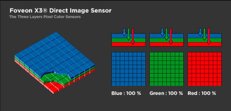
One of the more creative approaches for single chip colour image sensors is the brainchild of Carver Mead, a founding father of VLSI and microelectronics. In 2000, Foveon (www.foveon.com) introduced the X3 image sensor. This device achieves in a single chip what photographic film and 3-chip cameras had – complete RGB colour information at every pixel location. They do this by a very clever (and proprietary) imitation of a technique that was used for decades with great success in the photographic film industry – vertical stacking of photosensitive films. The difference is that what Kodak, Fuji and others did with silver-halide grains, Foveon does with colour-sensing pixels as shown in Figure 10.
 FIG 10The mechanism that is used in these sensors to enable vertical pixel stacking is that, in silicon, different wavelengths of light are absorbed at different depths. So, blue light with relatively short wavelengths is absorbed and converted into an electrical signal fairly close to the surface of an imaging array, green is absorbed a bit lower in the device, and red lower still. If the blue light-receiving surface of the sensor can be made thin enough and close enough to the surface, then the green and red components of an image can pass through the blue layer with very little attenuation to where their respective light-detecting pixels are located. If these overlapping pixel layers are designed and fabricated correctly, then complete RGB information can be obtained at every pixel in the array.
An image sensor design of this type plays directly to the strengths of silicon device design and wafer processing while avoiding the limitations of the Bayer pattern CFA approach. Because the inherent colour-filtering properties of silicon are used to separate colours, no additional colour filter array layers are required.
However, from the point of view of colour reproduction, the challenges for this type of sensor are significant. While it’s true that blue photons tend to get absorbed in this sensor near the surface and red photons get absorbed at a lower depth, the out-of-band colour rejection in this design is very weak, resulting in large amounts of optical crosstalk among the stacked pixels. In fact, in early devices the optical pixel crosstalk was so large that a simple 3 x 3 colour matrix was not sufficient to separate the RGB colour channels. It was only through some fairly sophisticated non-linear colour matrix operations that an image with a reasonable colour gamut could be produced. This aspect of these sensors continues to cause somewhat of a processing bottleneck that limits the useful domain of the Foveon sensors to digital still photography.
If the inherent colour separation properties of the sensor can be improved and/or the colour processing time required to obtain wide colour gamut images can be reduced, these may find an interesting application in video.
Conclusion
After reading this survey of colour image sensors, if you’ve come to the realisation that there is no clear winner in the technologies mentioned, then I’ve done my job. The 3-chip approach is the best today but may run out of steam as pixel sizes shrink; for single chip colour the venerable Bayer pattern is still not a perfect fit with existing semiconductor processing and non-Bayer approaches are still a bit of a long shot. I tend to compare the state of the art in colour image sensors today to where photographic film was in the first half of the 20th century. We have seen some real progress in this area in the last 20 years, but I believe the best is yet to be.
Matt Whalen is the founder and Chief Imaging Scientist for Applied Color Science, Inc. (www.appliedcolorscience.com) He has been actively involved in CMOS image sensor applications and digital image processing for over 10 years. His work in image sensor evaluation and image processing development has ranged from consumer products (AT&T’s Videophone, SiliconFilm’s eFilm cartridge, Kodak) to medical (Smith and Nephew HD endoscopy camera) to professional.
Whalen has held senior technical positions with Lucent/ Bell Labs, Conexant, and SiliconFilm Technologies. He currently holds more than 10 patents in the areas of lightwave and digital camera technology and has published numerous technical articles and conference papers in these areas. He has a B.S./M.S. in Physics from Rutgers University and is a member of the Society of Imaging Science and Technology.


